Overview
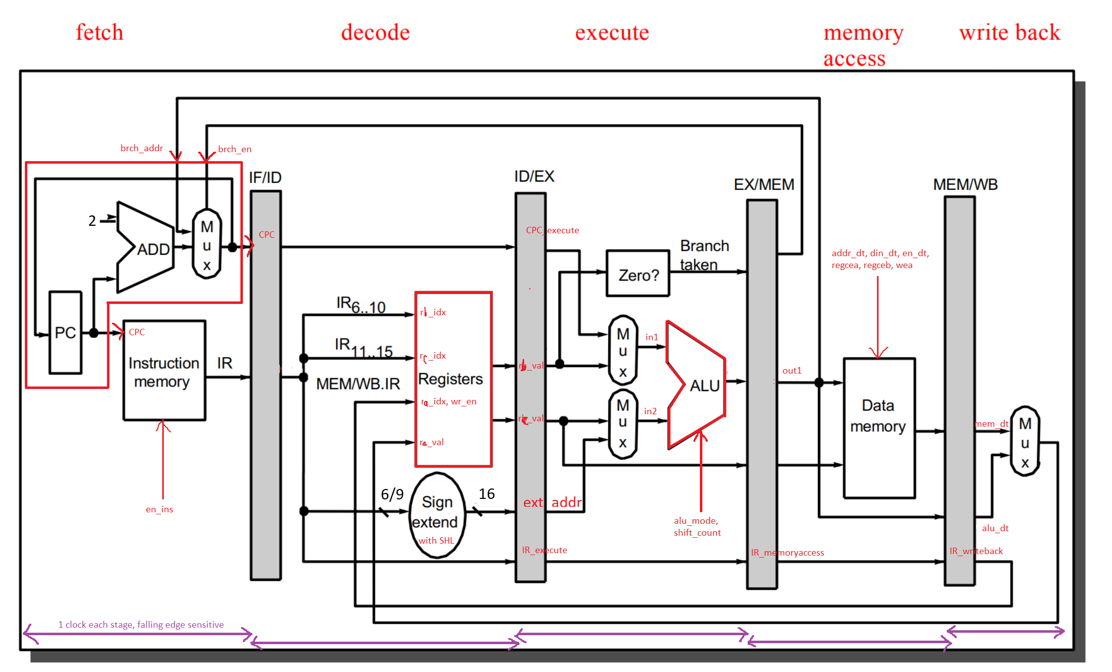
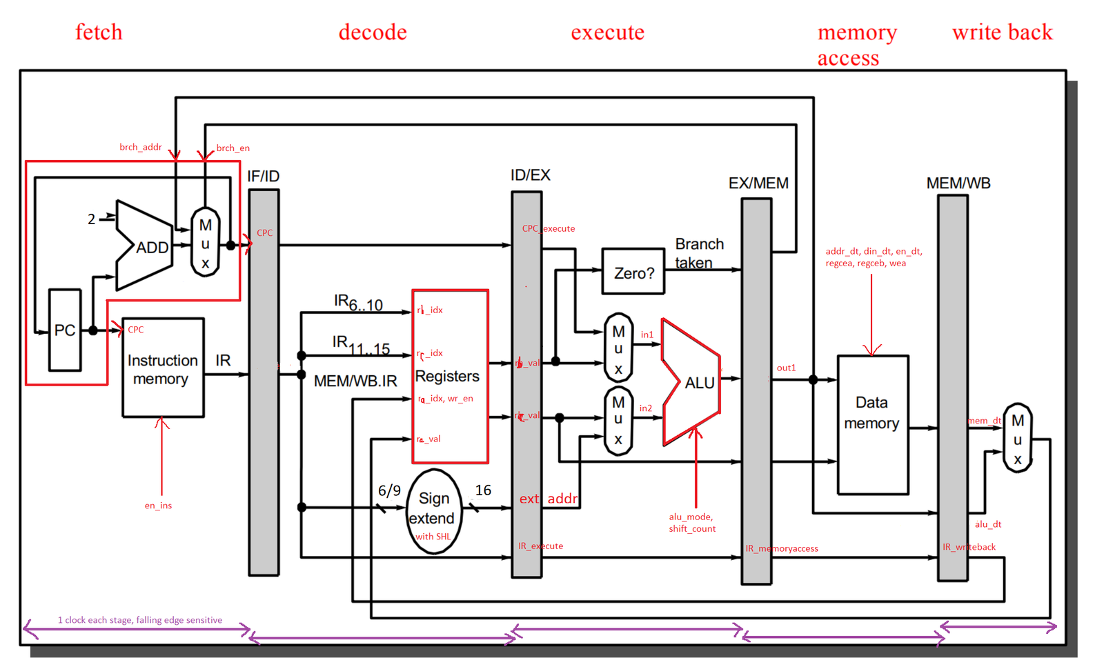
Built from the ground up in VHDL, the processor implements a 16-bit ISA with multiple instruction formats (three-register ALU operations, immediates, loads and stores, and branches) flowing through a classic pipeline with hazard handling. The design was synthesized in Xilinx Vivado and validated on real hardware rather than simulation alone.
The part that made debugging tractable: a VGA console rendered by the FPGA itself. A chain of formatting modules (nibble → byte → word to ASCII) streams register and memory state to a screen through a custom video-timing generator, so the processor's internals are visible live while programs run. A bootloader and memory-mapped I/O round out the system, letting programs load and interact with the board's switches and displays.
Highlights
- Complete datapath in VHDL: ALU, register file, program counter, sign extension, ROM/RAM, and forwarding/hazard logic.
- On-FPGA VGA debug console with custom video timing and hardware ASCII formatters.
- Bootloader plus memory-mapped I/O for the Nexys A7's peripherals, including the 7-segment display.
- Verified on hardware with Vivado's Integrated Logic Analyzer (ILA).